Fotosil – Photoluminescent ions for the formation of third generation photovoltaic cells based on silicon.
The FotoSil Project ‘Photoluminescent ions for the formation of third generation silicon-based photovoltaic cells’ was funded by the Ministry of Science and Innovation, within the National Plan for Scientific Research, Development and Technological Innovation, 2008-2011, Sub-programme for scientific and technological actions in Science and Technology Parks, INNPLANTA 2011. The total grant amounted to €808,088.00 (2011-2013), 70% of which came from the European Regional Development Fund (ERDF) of the European Commission.
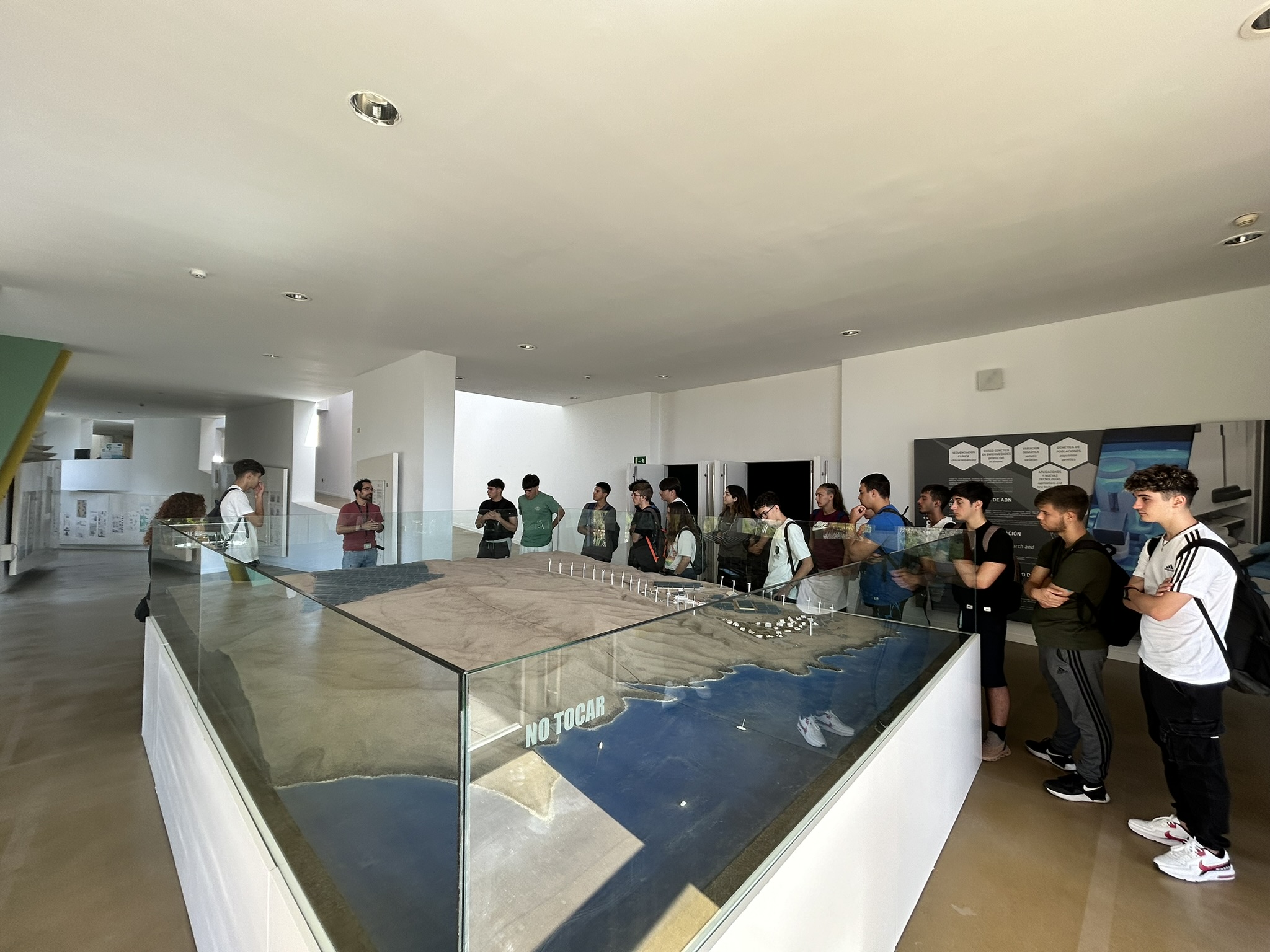
Solar photovoltaic energy is one of the renewable energies that is in continuous evolution, a basic issue to optimise is the development of more efficient and cheaper photovoltaic cells. Achieving these improvements in technology is a key issue in order to favour the large-scale integration of this energy.
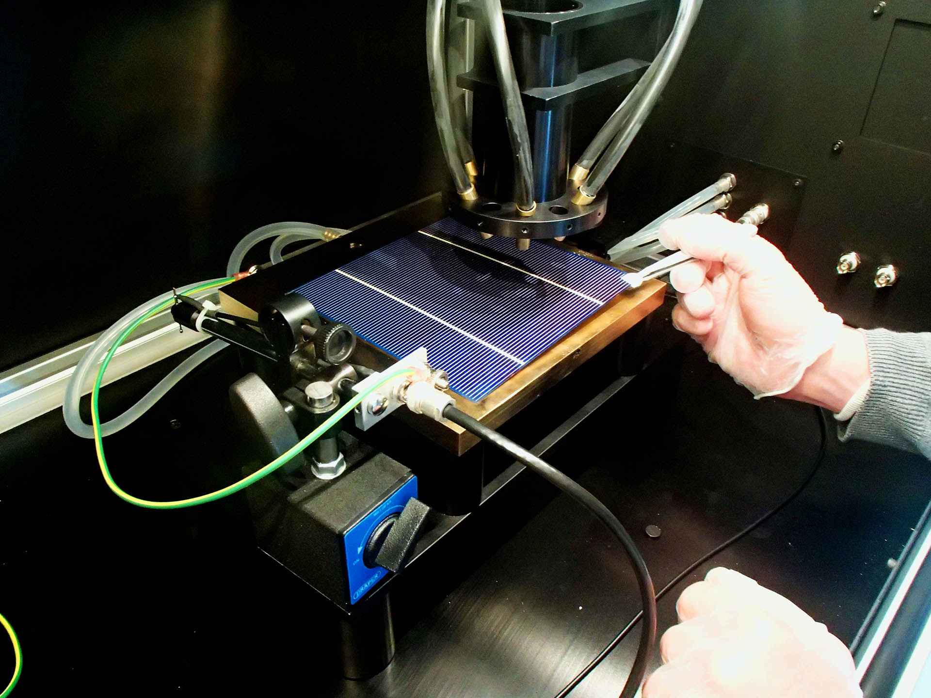
The overall objective of the FotoSil project was to manufacture more efficient, low-cost silicon photovoltaic cells using third-generation cell technology in order to improve photon absorption and obtain more efficient emitters.
To achieve this goal, it was necessary to develop different processes and technologies. Firstly, to develop processes for the manufacture of high-efficiency photovoltaic cells that also reduce production costs. To this end, the processes for the formation of photovoltaic cells on monocrystalline substrates were analysed in order to try to transfer and adapt these processes to multicrystalline substrates. Currently, most photovoltaic cells are manufactured on multicrystalline substrates because, although these are of lower quality than monocrystalline substrates, they are cheaper.
Next, Develop the process of obtaining more efficient emitters. Having more efficient emitters would lead to an electrical improvement in the photovoltaic cell. This improvement was approached from two starting points, on the one hand the use of amorphous silicon sheets on textured surfaces and on the other the use of selective emitters under the metal contacts to favour current generation. And finally, to develop intrinsic amorphous silicon film deposition processes. The aim was to create an amorphous silicon interlayer in order to improve the emitter response to the most energetic photons in the UV-VIS range.
In addition to improving and developing processes, work was also done on the development of third-generation cell technology. To this end, the behaviour of photoluminescent materials such as rare earths and silicon nanostructures was studied to act jointly as photoconverters, in order to increase the efficiency of photoconversion, and therefore the performance of the cell.